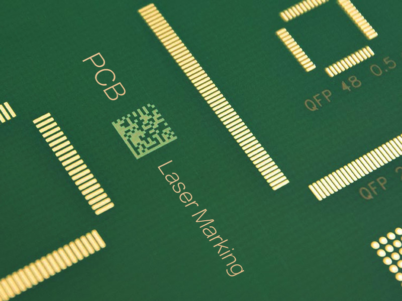
The electronics industry sees unprecedented transformation. Laser marking of circuit boards stands as a cornerstone tech. It meets precision, efficiency, & traceability demands on modern manufacturing. From smartphones to electric vehicles, nearly every electronic device relies on printed circuit boards (PCBs). These need permanent identification for quality control & supply chain management. Laser marking technology becomes industry standard. It outperforms traditional marking methods. It also supports automation & sustainability drives.
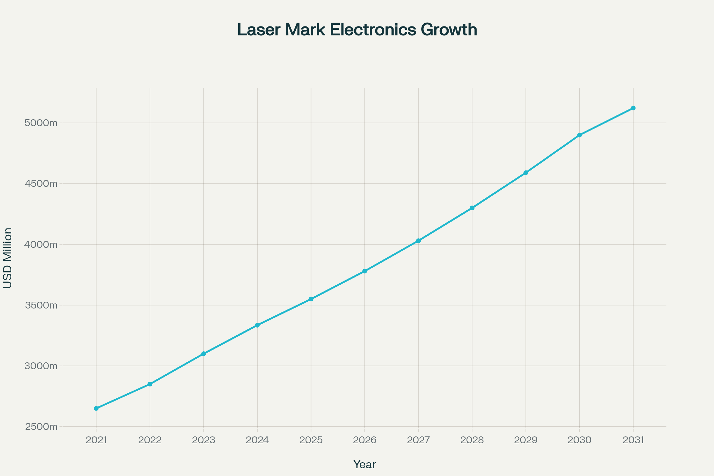
The global electronics industry is one of an world’s largest manufacturing sectors. The laser marking market in electronics alone is projected to grow from $3.33 billion on 2024 to $5.12 billion by 2031. This is a compound annual growth rate (CAGR) of 6.3%. Such growth reflects electronic devices’ increasing complexity. It also shows the need for precise identification & traceability systems.

Over past two decades, electronics manufacturing landscape evolved drastically. Modern electronic components grow increasingly miniaturized. They also grow more sophisticated. Manufacturing processes must maintain precision at microscopic scales. Traditional marking methods like ink printing & adhesive labels fall short in these demanding apps. Especially when components face harsh conditions or need long - term readability.
Laser marking tech offers transformative advantages. It becomes indispensable in electronics manufacturing. The non - contact nature of laser processing eliminates mechanical stress on sensitive components. Focused laser beams’ precision enables marking at resolutions impossible with conventional methods.

The tech’s versatility covers multiple materials in electronics manufacturing. This includes plastics, metals, ceramics, & specialized substrates. UV Laser systems, operating at 355 nanometers, work well for marking flame - retardant materials on electronic housings. They achieve high contrast markings via photochemical reactions, not thermal processes.
In electronics industry, traceability is not just a convenience. It’s a critical business requirement. When manufacturing defects happen, companies must quickly identify & isolate affected products. This prevents widespread quality issues & safety hazards. Laser - marked identification codes — 2D matrix codes, QR codes, alphanumeric sequences — link individual circuit boards to their manufacturing data.
Laser markings’ permanence solves a key limitation of traditional labeling methods. Unlike adhesive labels that peel off or ink markings that fade, laser markings stay legible through a product’s lifecycle. Even when exposed to extreme temps, chemicals, or mechanical wear. This durability matters for products in service for decades, like automotive electronics or industrial control systems.
Laser marking’s economic advantages show when comparing cost structures with traditional methods. Industry data shows laser marking costs around $0.02 per marking. This is much lower than ink - based systems’ $0.07 - 0.09 per marking. This cost difference adds up in high - volume production, saving manufacturers much.
Beyond direct cost savings, laser marking systems boost operational efficiency via automation. Modern laser marking stations integrate into SMEMA - compliant production lines. They enable continuous processing without manual intervention. The systems can mark both sides of circuit boards at once. They also have automated quality verification features. These read & validate marked codes before products move to next production stage.
PCB laser marking has multiple technical approaches. These are tailored to different substrate materials & app requirements. For standard FR - 4 substrates with solder mask coatings, CO2 lasers operating at 10.6 micrometers offer good marking contrast. They do this via controlled ablation of the surface layer.
UV Laser systems gain popularity for marking sensitive electronic components. Especially those with flame - retardant materials. The 355 - nanometer wavelength of UV Lasers enables “cold marking” processes. These achieve high contrast without excess heat that could damage surrounding components. This is vital when marking near temperature - sensitive components or working with materials with low thermal damage thresholds.

The semiconductor industry poses unique laser marking challenges. This is due to microscopic dimensions & high component value. Diode laser systems provide the precision needed for marking individual semiconductor packages. They also stay gentle enough to avoid damaging underlying silicon structures.
In semiconductor apps, laser marking has functions beyond identification. It enables wafer dicing via precise scribing, surface preparation for wire bonding, & alignment mark creation for subsequent steps. Laser processing’s non - contact nature is valuable in cleanroom environments where contamination control is key.
The electronics industry’s adoption of advanced materials drives laser marking tech developments. Flame - retardant synthetic materials — used in switch housings & connector bodies — need specific wavelength selection for optimal marking. UV Lasers work best here, creating markings via photochemical reactions instead of thermal processes.
Glass & ceramic substrates, used more in high - frequency apps & LED packaging, bring technical challenges. UV Laser systems can mark these materials without inducing thermal stress that causes cracking or optical distortion. Precise pulse energy & duration control lets manufacturers achieve required marking depth while keeping material integrity.
The laser marking industry evolves rapidly. Demands for more automation, higher precision, & wider material compatibility drive this. Recent innovations include AI - supported parameter optimization. These systems automatically determine optimal laser & lighting settings for different materials & apps. They cut setup time & improve marking consistency across production runs.
Machine learning algorithms integrate into quality control systems. They enable automated defect detection & process optimization. These systems spot potential marking issues before they hurt product quality. This reduces waste & improves overall equipment effectiveness.
Modern laser marking systems integrate well with Industry 4.0 manufacturing concepts. They use standardized communication protocols like IPC - HERMES - 9852, IPC - CFX, & OPC UA. These enable real - time data exchange between marking systems & higher - level manufacturing execution systems. This supports comprehensive traceability in production.
Integration extends to predictive maintenance systems. These monitor laser performance parameters & predict component replacement needs before failures. This proactive approach cuts unplanned downtime. It also ensures consistent marking quality through system lifecycles.
Environmental sustainability drives laser marking tech development. Laser systems eliminate the need for chemical consumables in ink - based marking. This cuts operational costs & environmental impact. Laser processing’s precision also reduces material waste via accurate energy delivery & less rework.
Energy efficiency is a focus. Newer laser systems have sleep - mode for lower power use during production breaks. Advanced fume extraction systems keep production air clean. They also capture & process particulates generated during marking.
Laser marking of circuit boards has moved from an alternative to an essential manufacturing capability. It enables the electronics industry’s growth & innovation. The tech’s mix of precision, durability, & cost - effectiveness makes it indispensable for modern manufacturing. These operations need comprehensive traceability & quality control.
Market projections showing 93% growth over the next decade reflect rising electronic device demand. They also show more sophisticated manufacturing requirements. As electronic components keep miniaturizing & manufacturing automates more, laser marking tech will play a bigger role in enabling these advances.
The integration of artificial intelligence, advanced materials compatibility, & Industry 4.0 connectivity makes laser marking systems key enablers of future manufacturing. Companies investing in advanced laser marking tech today position themselves to capitalize on the global electronics market’s expansion. They also meet stricter product traceability & quality assurance requirements.
The shift from traditional to laser - based marking is more than a tech upgrade. It shows the electronics industry’s commitment to precision, sustainability, & manufacturing excellence. As the industry evolves rapidly, laser marking of circuit boards will stay at the forefront of enabling modern electronics manufacturing.
Contact: Jason
Phone: +8613337332946
E-mail: [email protected]
Add: Hangzhou City, Zhejiang Province, China